×
模态框(Modal)标题
在这里添加一些文本
Close
Close
Submit
Cancel
Confirm
×
模态框(Modal)标题
×
Home
About Journal
About Journal
Indexed in
Awards
Editorial Board
Guide for Authors
Browse
Current Issue
Just Accepted
Archive
Highlights
Topic
Most Viewed
Most Download
Most Cited
E-mail Alert
RSS
Subscribe
Download
Editorial Policy
Contact Us
Figure/Table detail
Research and implementation of clock system for automotive electronic MCU
FU Jianjun, BAO Yipeng, JIANG Hequan
Integrated Circuits and Embedded Systems
, 2025, 25(
7
): 73-79. DOI:
10.20193/j.ices2097-4191.2025.0014
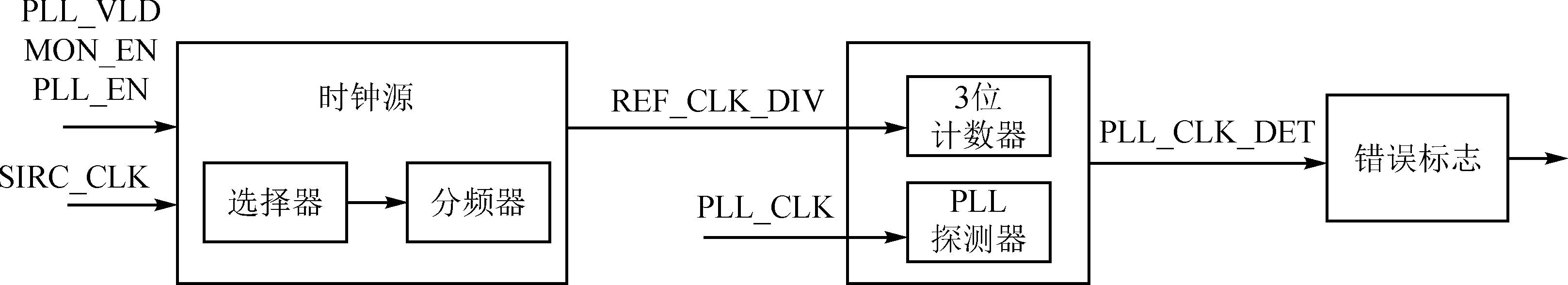
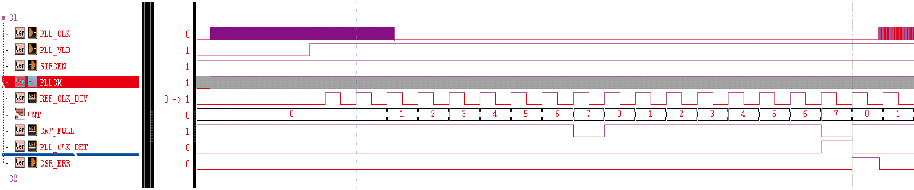
Fig. 8
Schematic diagram of PLL clock monitor structure
Other figure/table from this article
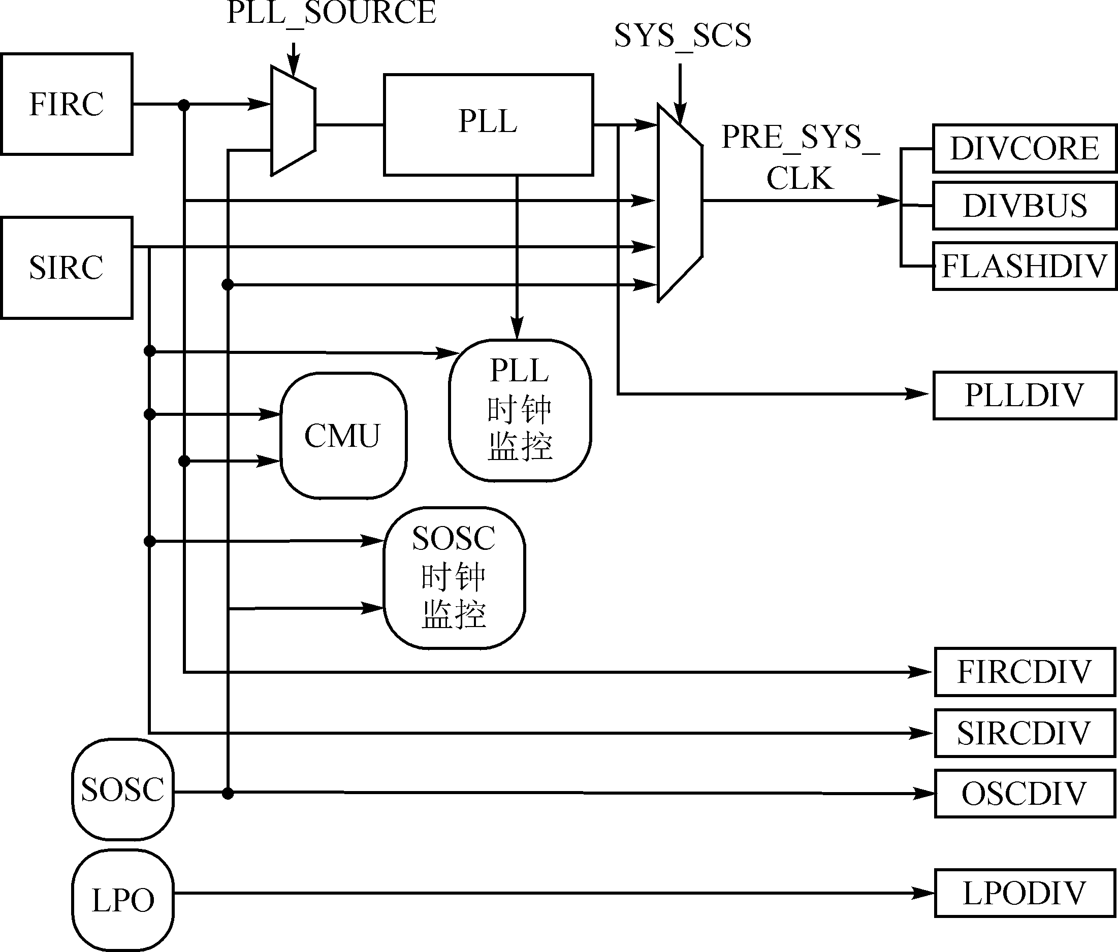
Fig. 1
Clock architecture diagram of automotive electronic MCU
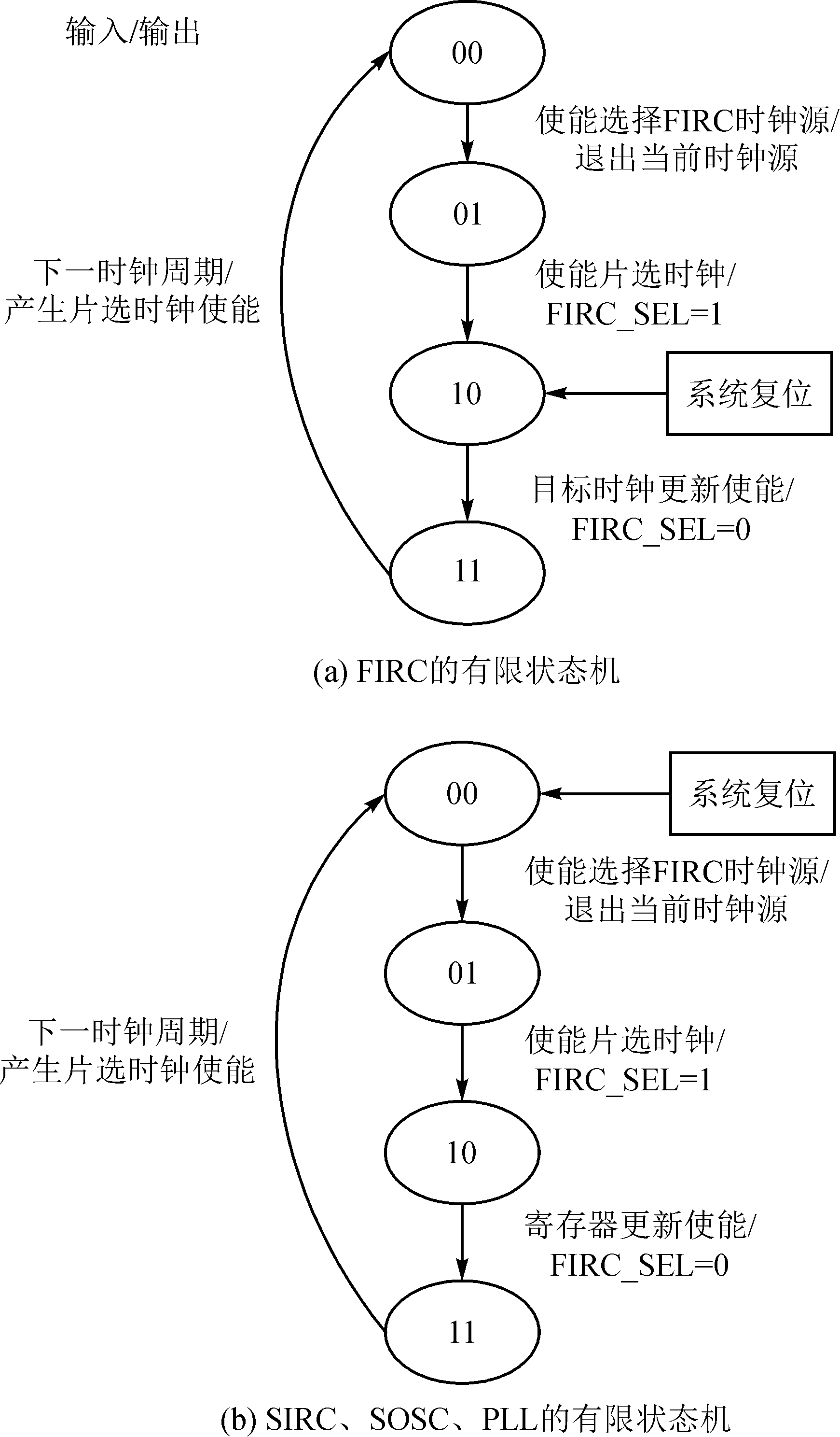
Fig. 2
Clock source switching
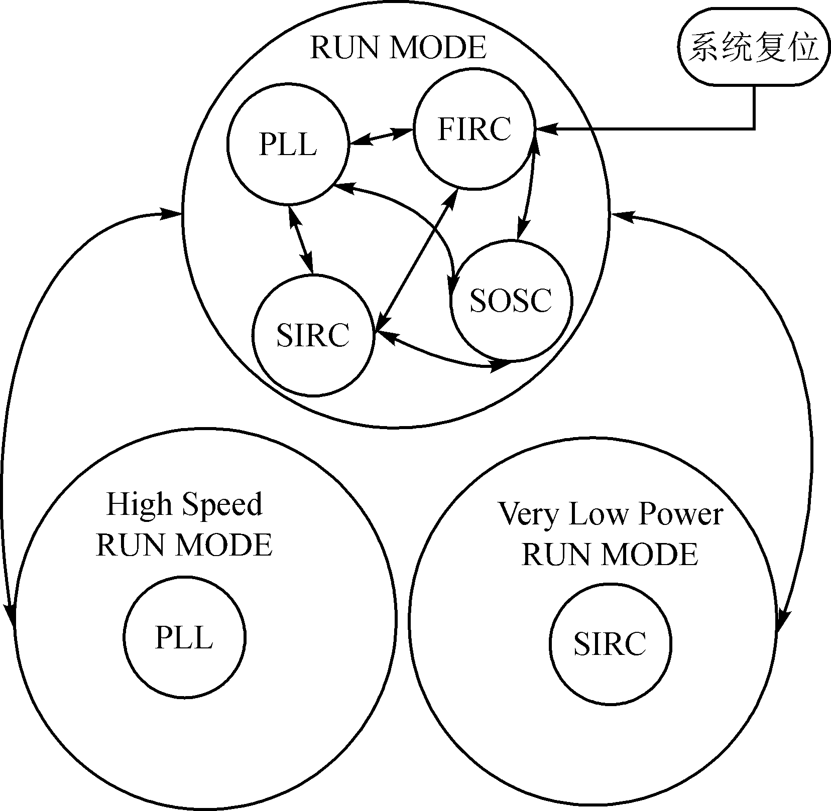
Fig. 3
Relationship between operating mode and system clock selection
Table 1
Safe operating frequency of internal clock(unit:MHz)
Fig. 4
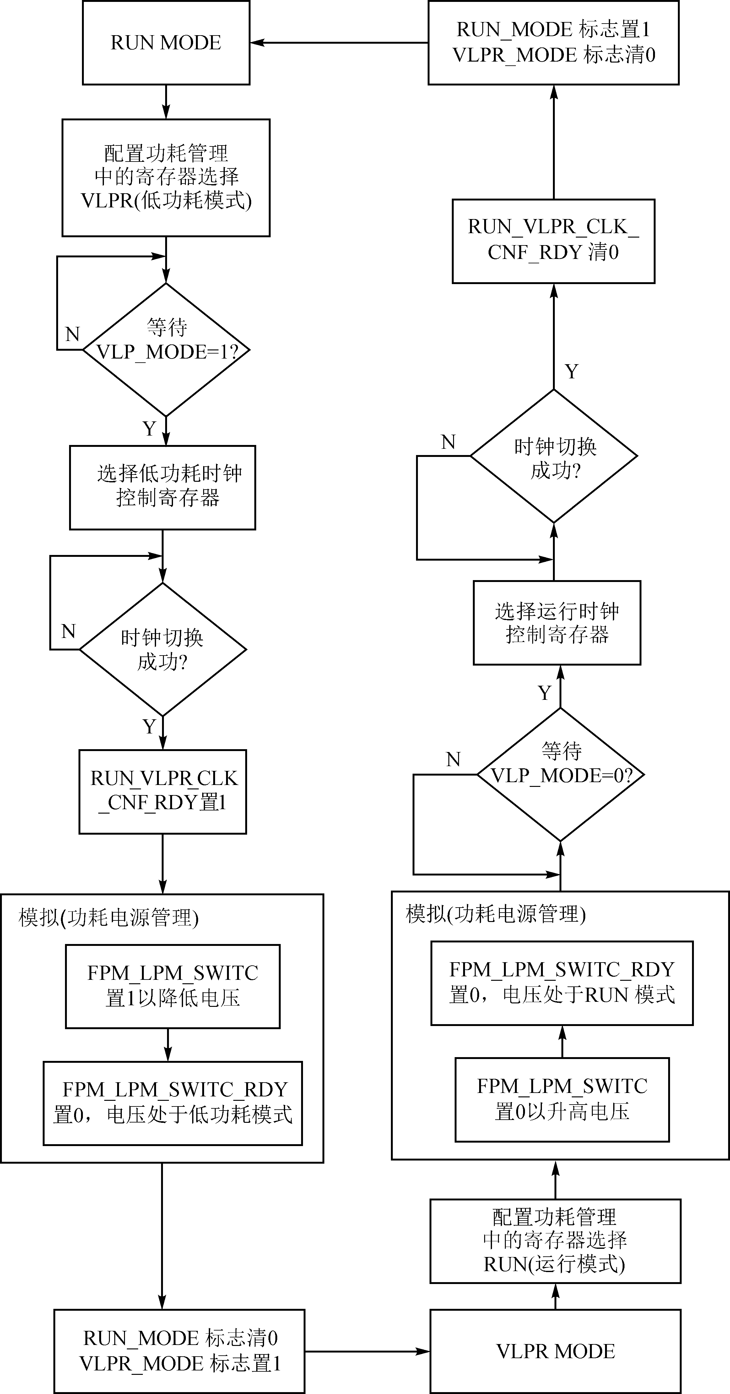
Switching process between RUN mode and VLPRUN mode
Fig. 5
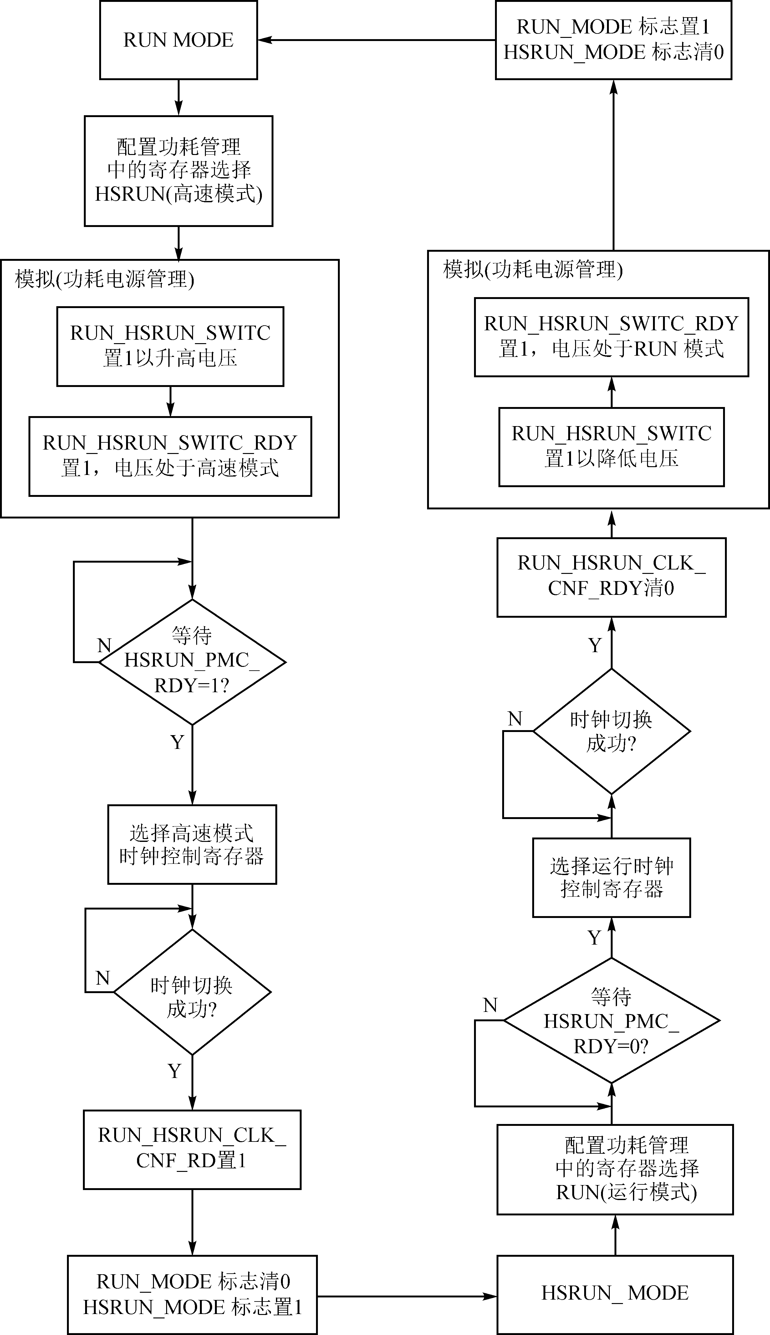
Switching process between RUN mode and HSRUN mode
Fig. 6
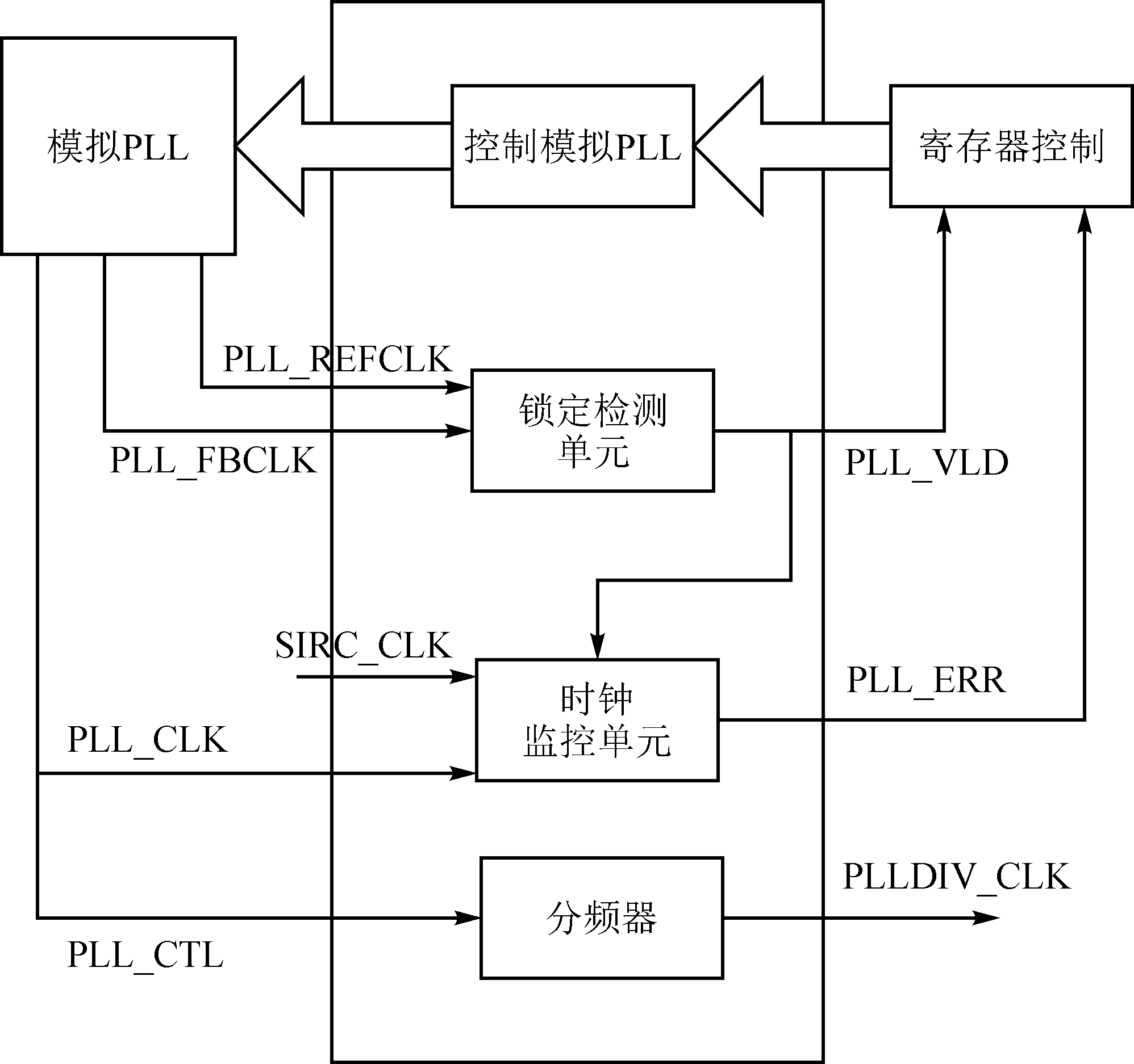
PLL control block diagram
Fig. 7
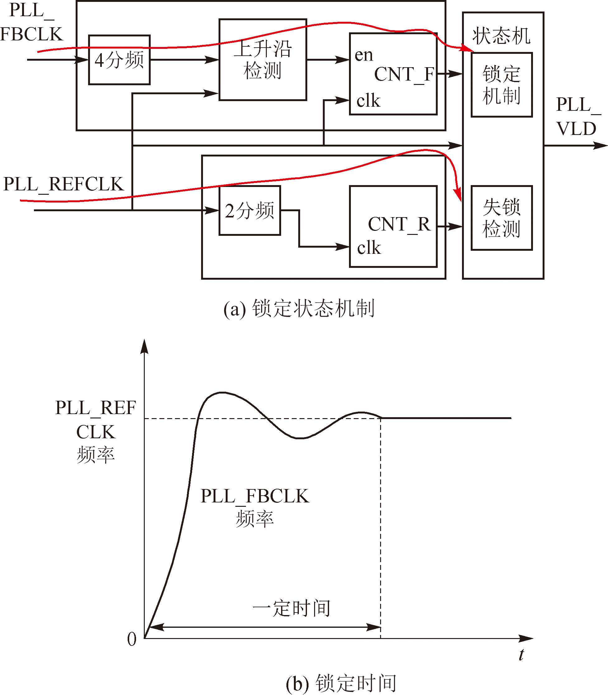
Lock state mechanism and lock time
Fig. 9
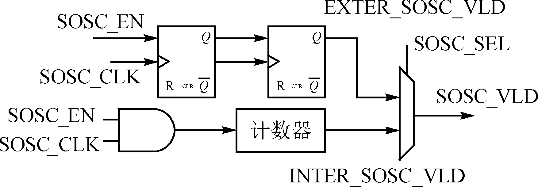
Circuit diagram of SOSC effective signal generation
Fig. 10
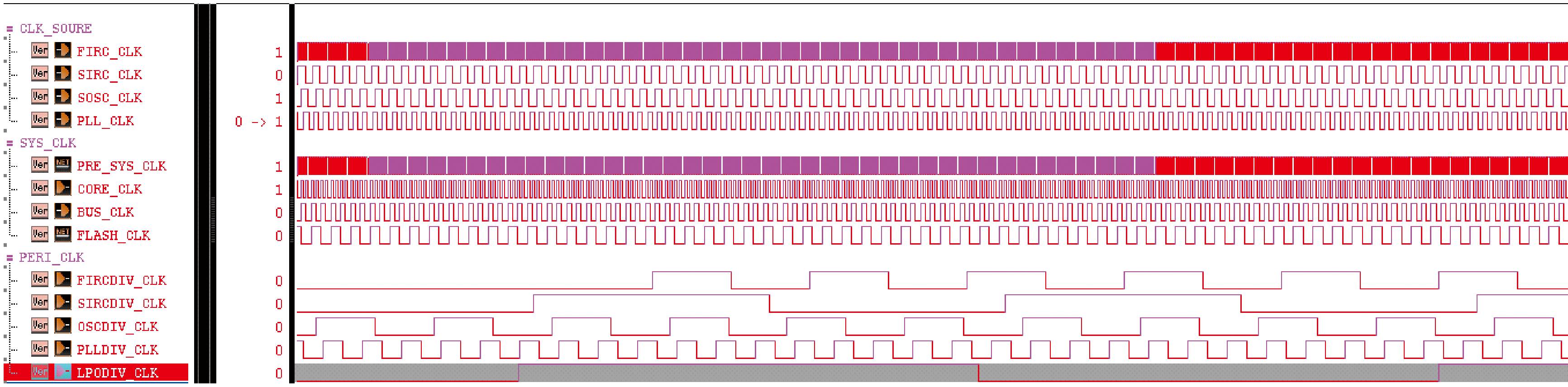
Clock distribution simulation diagram
Fig. 11
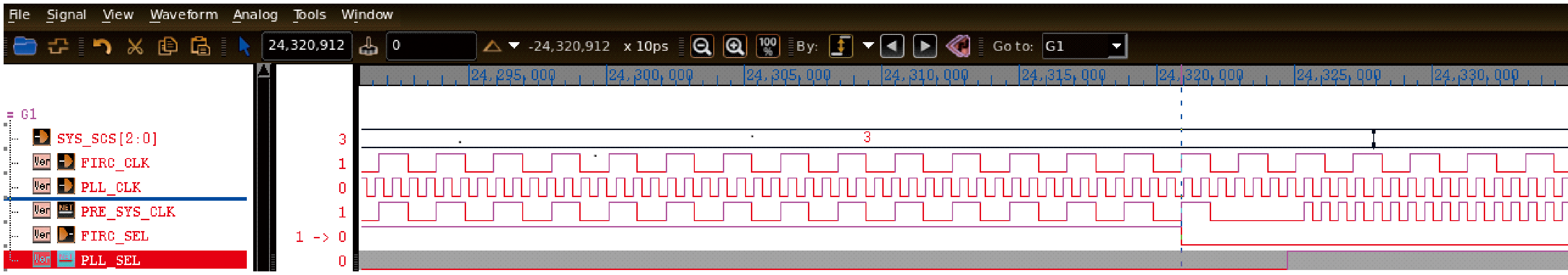
Simulation diagram of clock source switching
Fig. 12
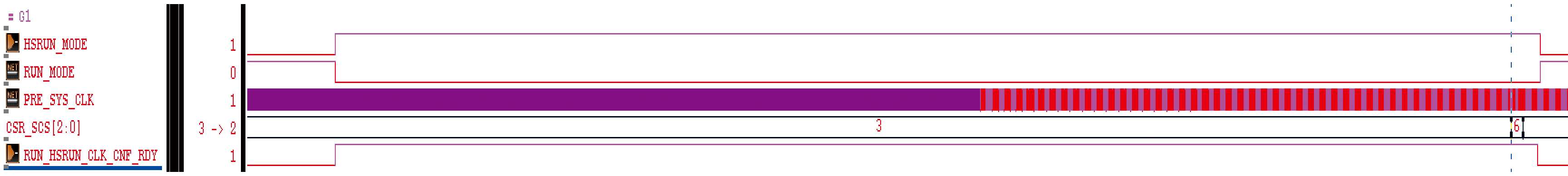
Simulation diagram of power switching
Fig. 13
PLL clock monitoring diagram