×
模态框(Modal)标题
在这里添加一些文本
Close
Close
Submit
Cancel
Confirm
×
模态框(Modal)标题
×
Home
About Journal
About Journal
Indexed in
Awards
Editorial Board
Guide for Authors
Browse
Current Issue
Just Accepted
Archive
Highlights
Topic
Most Viewed
Most Download
Most Cited
E-mail Alert
RSS
Subscribe
Download
Editorial Policy
Contact Us
Figure/Table detail
Research and implementation of clock system for automotive electronic MCU
FU Jianjun, BAO Yipeng, JIANG Hequan
Integrated Circuits and Embedded Systems
, 2025, 25(
7
): 73-79. DOI:
10.20193/j.ices2097-4191.2025.0014
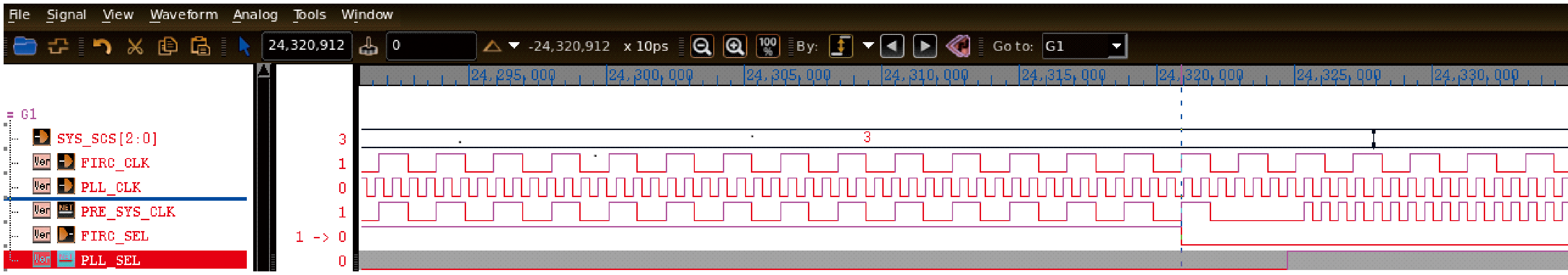
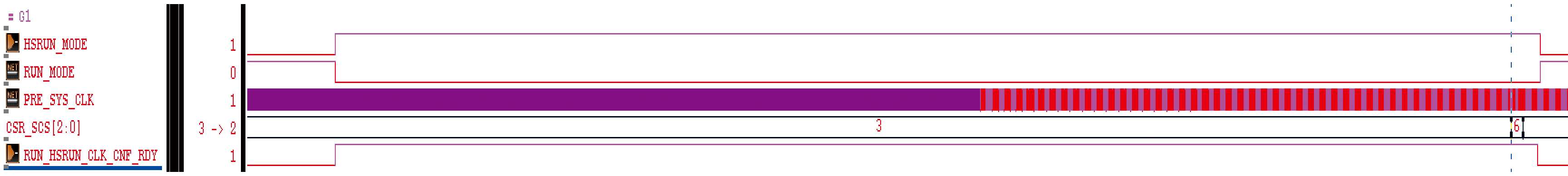
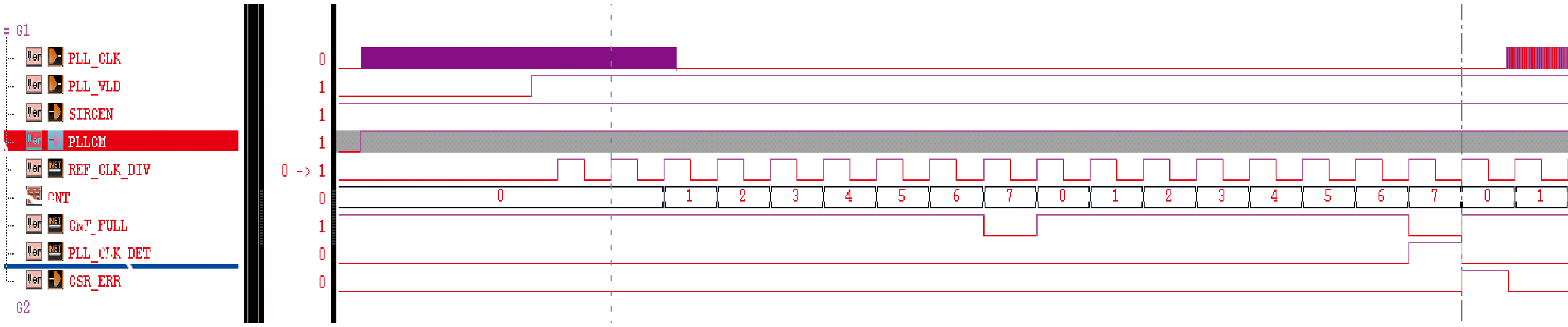
Fig. 11
Simulation diagram of clock source switching
Other figure/table from this article
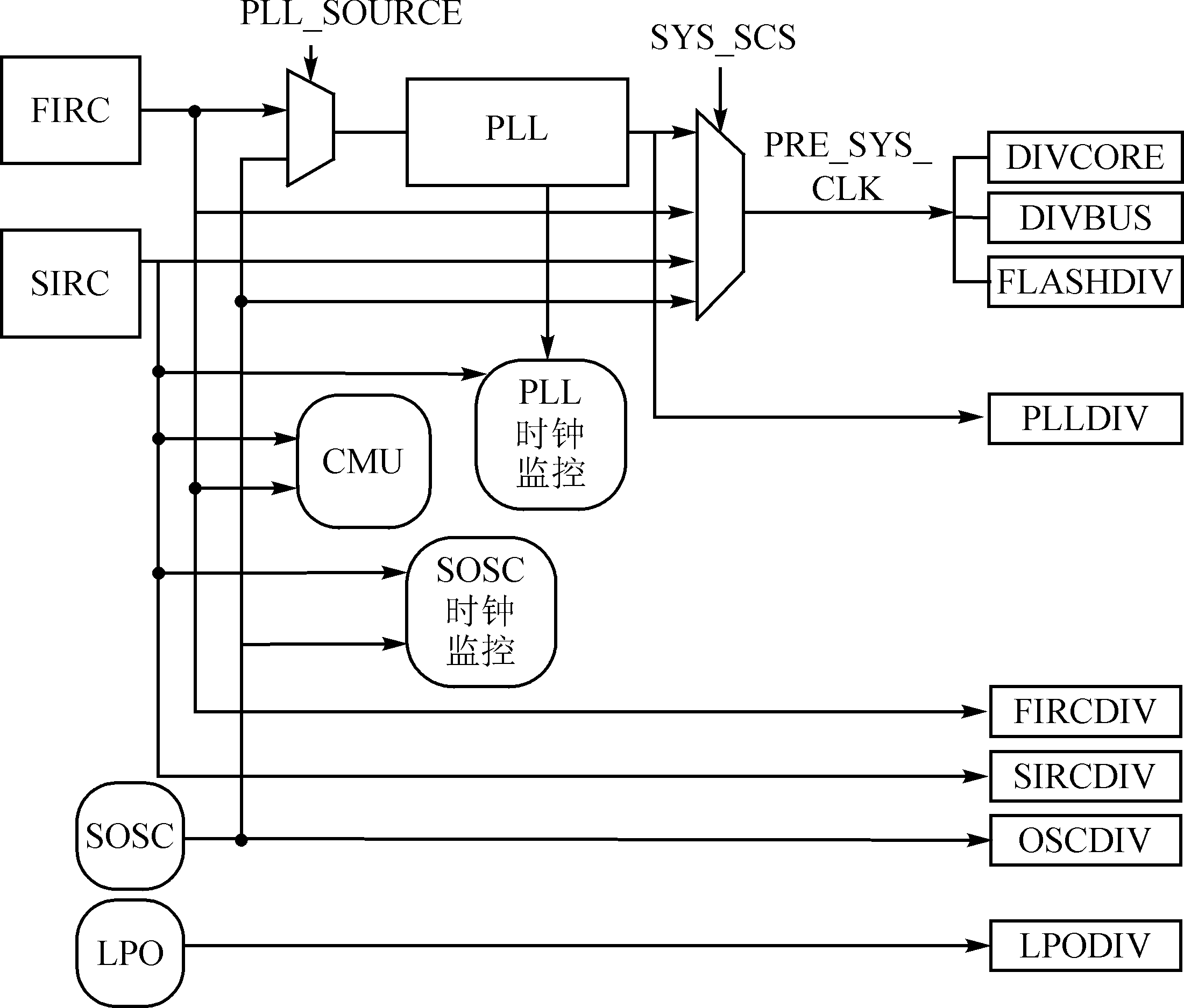
Fig. 1
Clock architecture diagram of automotive electronic MCU
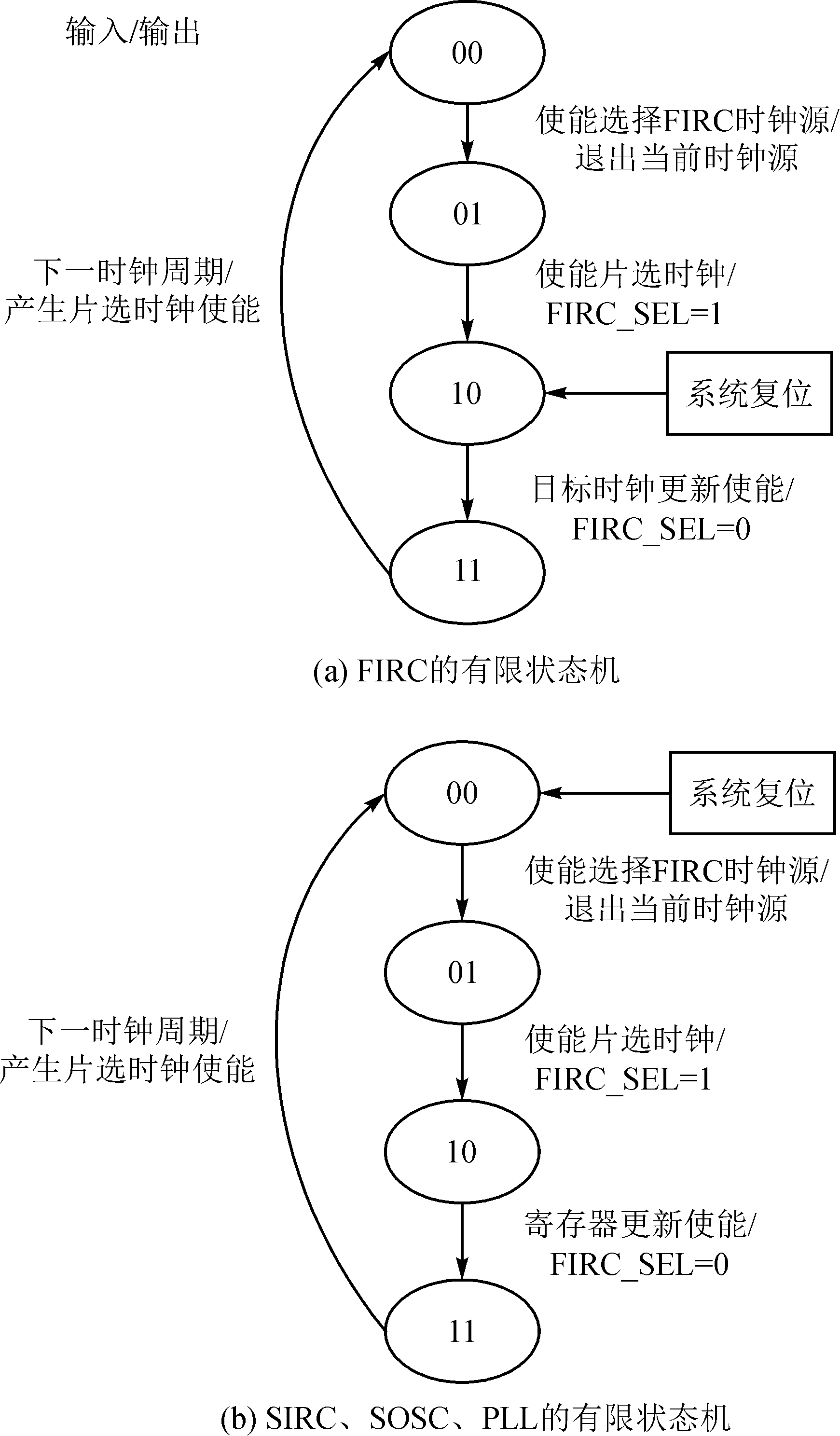
Fig. 2
Clock source switching
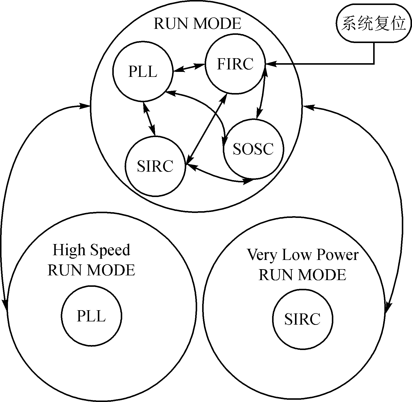
Fig. 3
Relationship between operating mode and system clock selection
Table 1
Safe operating frequency of internal clock(unit:MHz)
Fig. 4
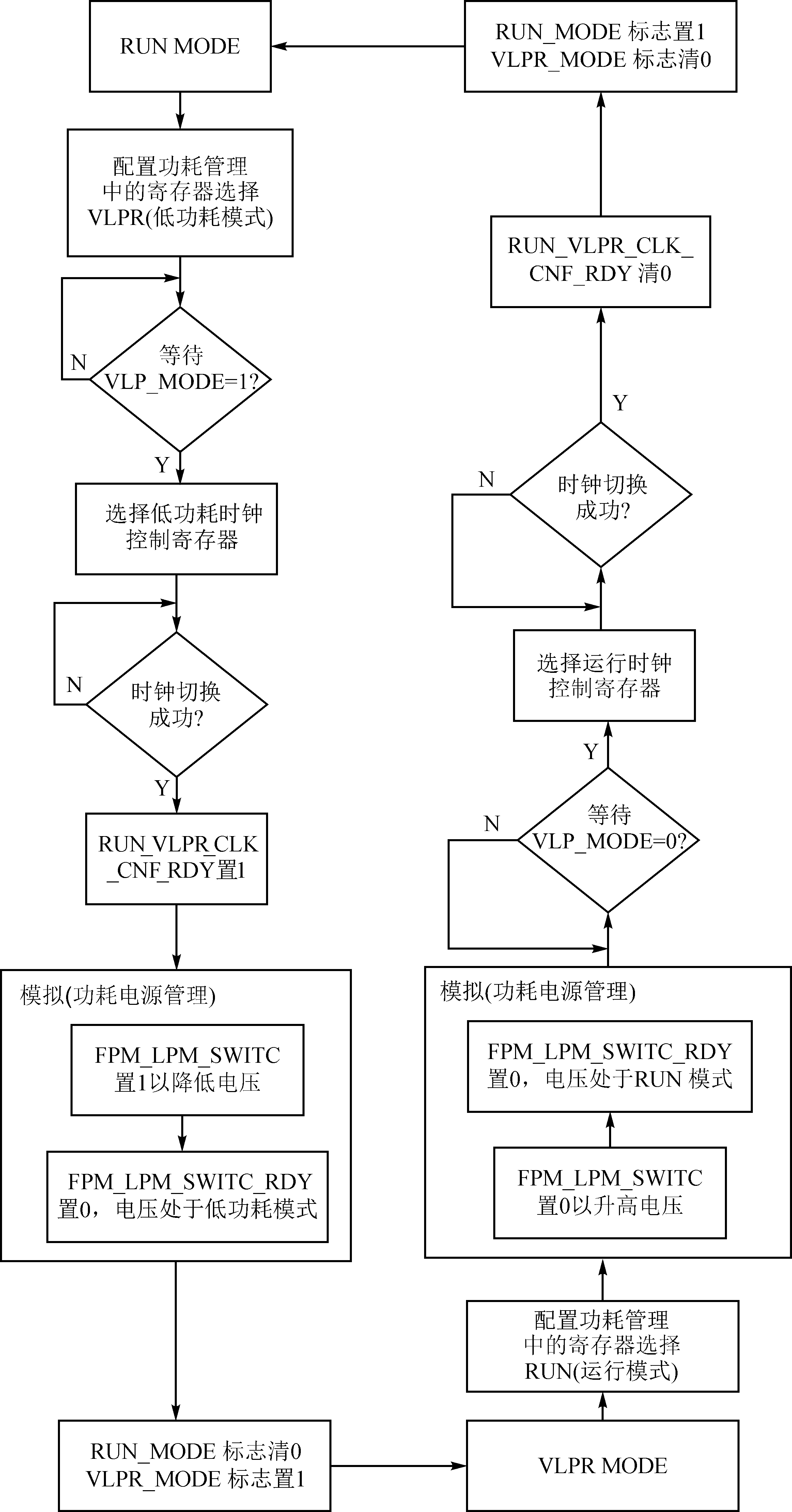
Switching process between RUN mode and VLPRUN mode
Fig. 5
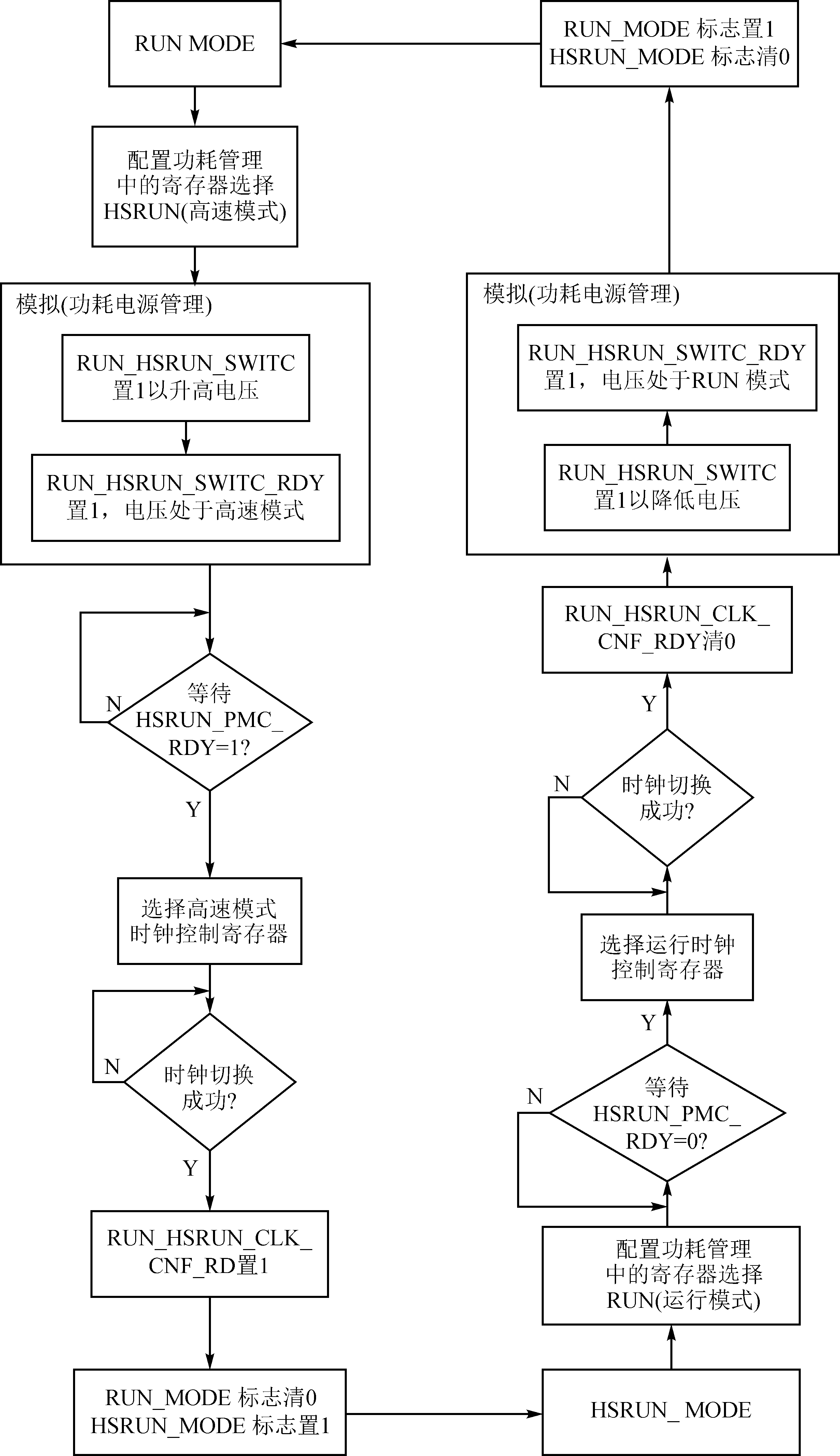
Switching process between RUN mode and HSRUN mode
Fig. 6
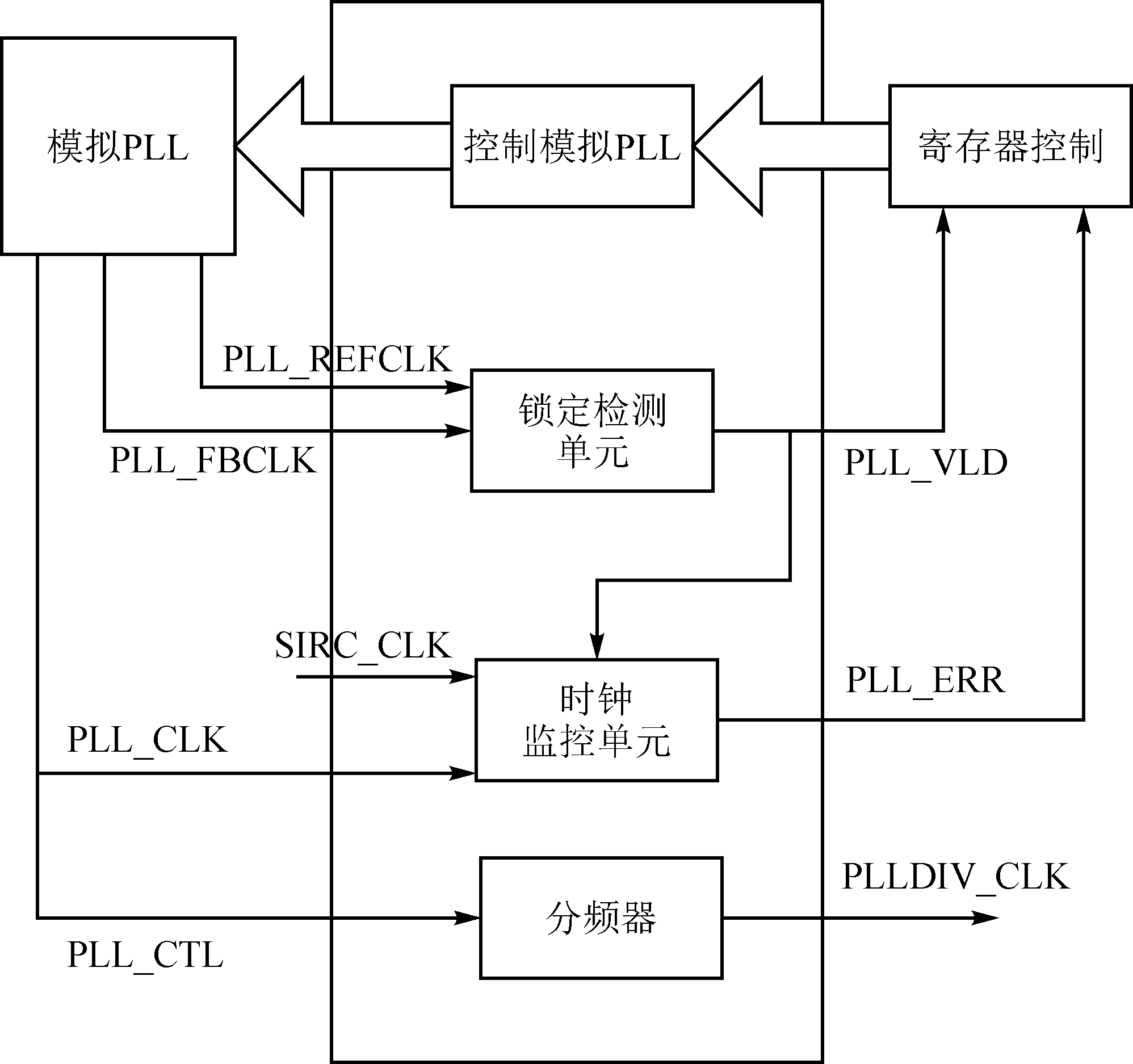
PLL control block diagram
Fig. 7
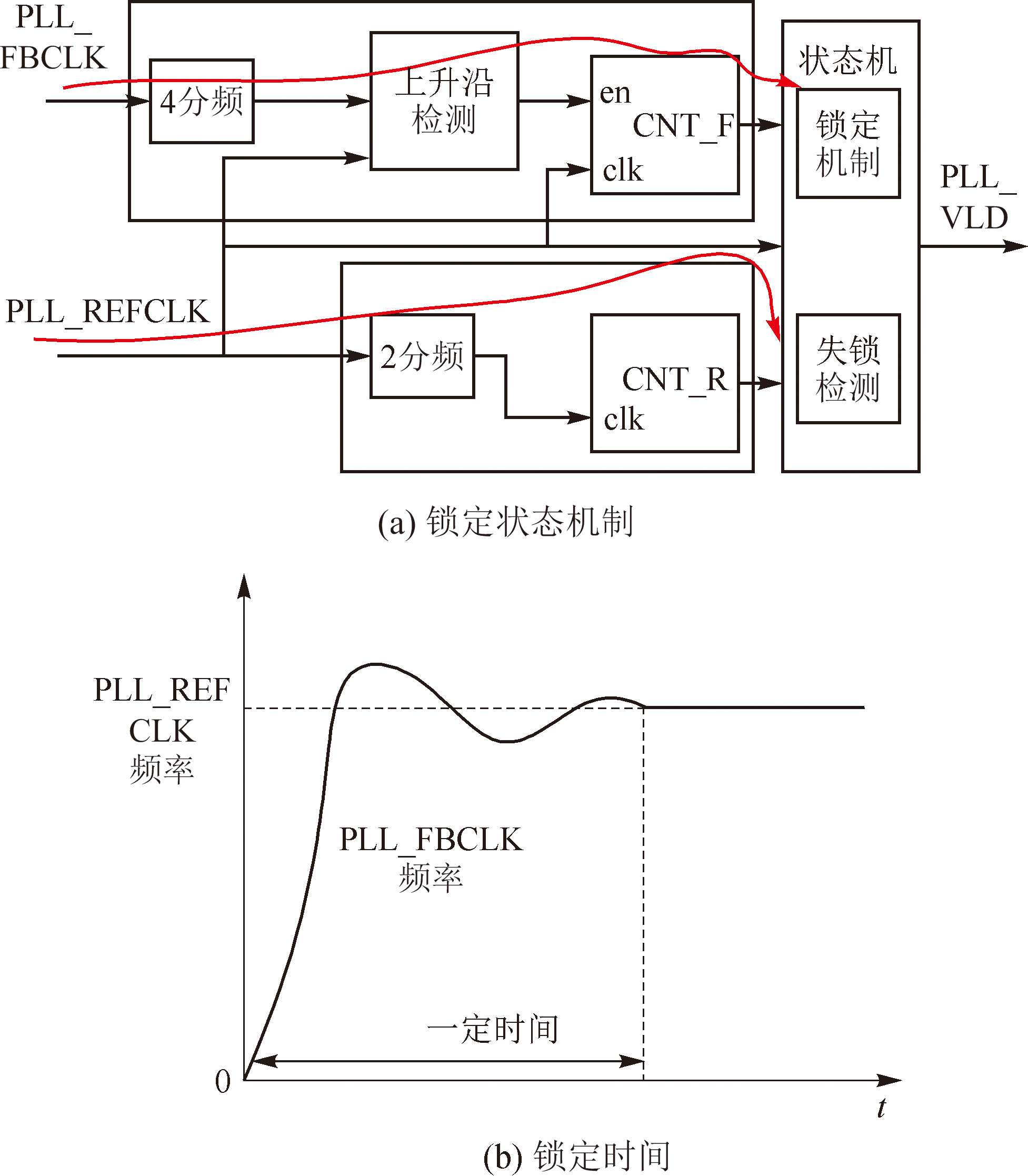
Lock state mechanism and lock time
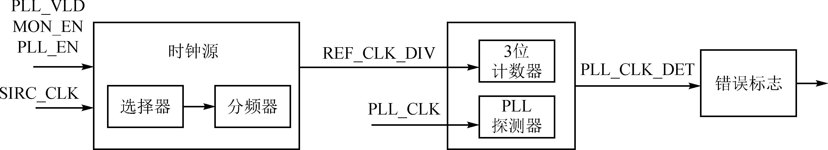
Fig. 8
Schematic diagram of PLL clock monitor structure
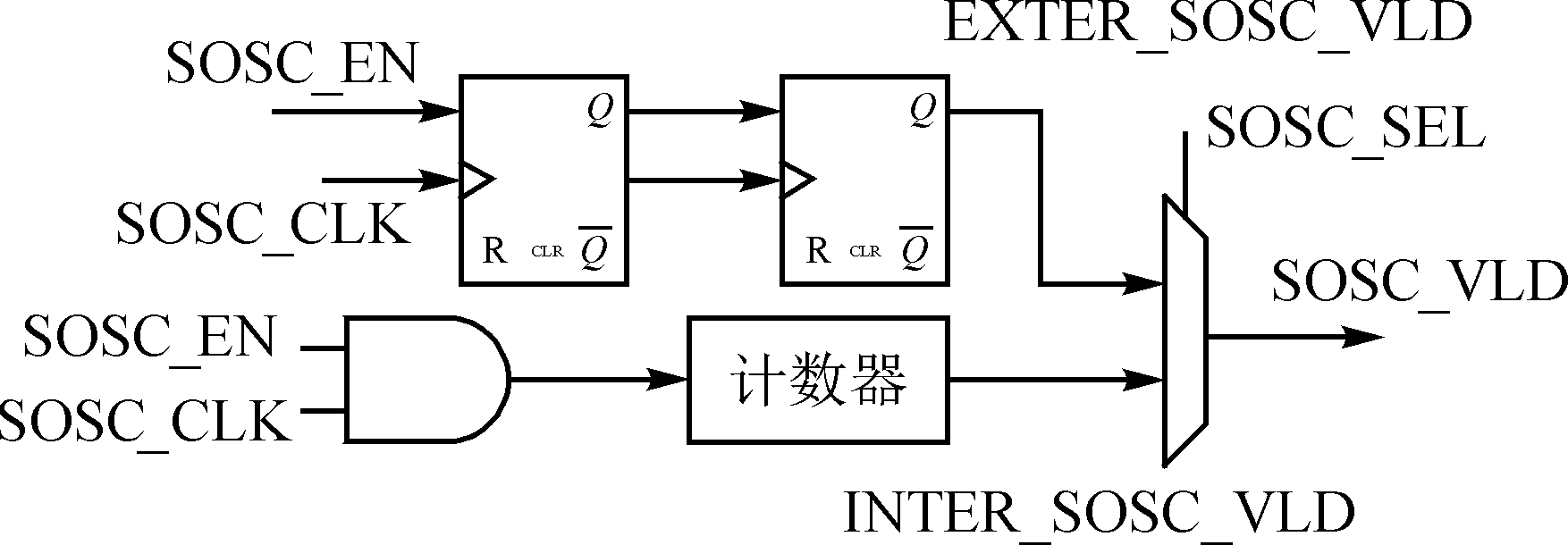
Fig. 9
Circuit diagram of SOSC effective signal generation
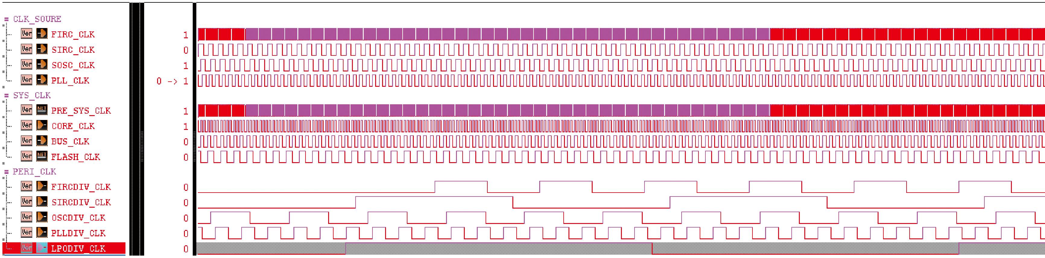
Fig. 10
Clock distribution simulation diagram
Fig. 12
Simulation diagram of power switching
Fig. 13
PLL clock monitoring diagram