×
模态框(Modal)标题
在这里添加一些文本
Close
Close
Submit
Cancel
Confirm
×
模态框(Modal)标题
×
Home
About Journal
Editorial Board
Guide for Authors
Browse
Current Issue
Just Accepted
Archive
Highlights
Topic
Most Viewed
Most Download
Most Cited
Subscribe
Download
Editorial Policy
Publication Ethics Statement
Peer Review Policy
Contact Us
中文
Figure/Table detail
Bias voltage and temperature dependence of single-event transient in 22 nm FDSOI devices
HUANG Xiaofeng, LI Chenming, WANG Haibin, SUN Yongshu, WANG Liang, GUO Gang, WANG Xueming
Integrated Circuits and Embedded Systems
, 2024, 24(
7
): 30-36.
工艺参数
数值
沟道长度
22 nm
沟道宽度
80 nm
源/漏掺杂浓度
3.5×10
19
cm
-3
源/漏轻掺杂浓度
3×10
16
cm
-3
体区掺杂浓度
5×10
15
cm
-3
埋氧层厚度
20 nm
栅氧化层厚度
1.25 nm
体区硅膜厚度
6 nm
外延层总厚度
16 nm
Table 1
22 nm FDSOI NMOS model process parameters
Other figure/table from this article
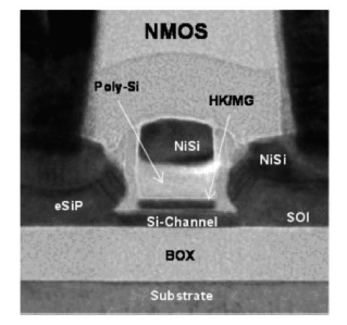
Fig. 1
Typical cross-section of 22 nm FDSOI NMOS
[
9
]
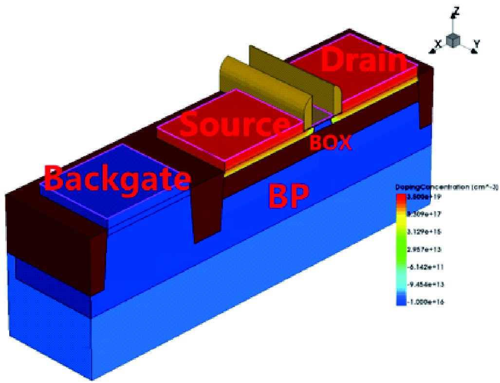
Fig. 2
22 nm FDSOI NMOS model
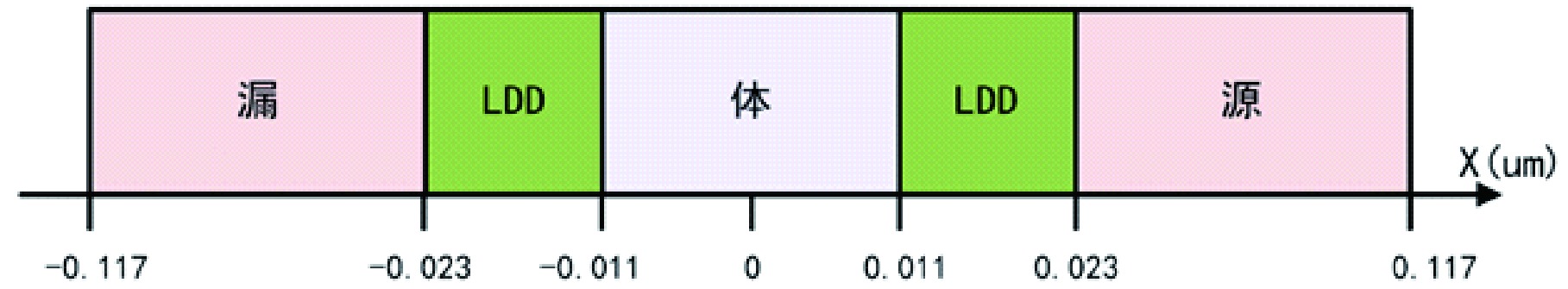
Fig. 3
Diagram of different positions in 22 nm FDSOI NMOS model
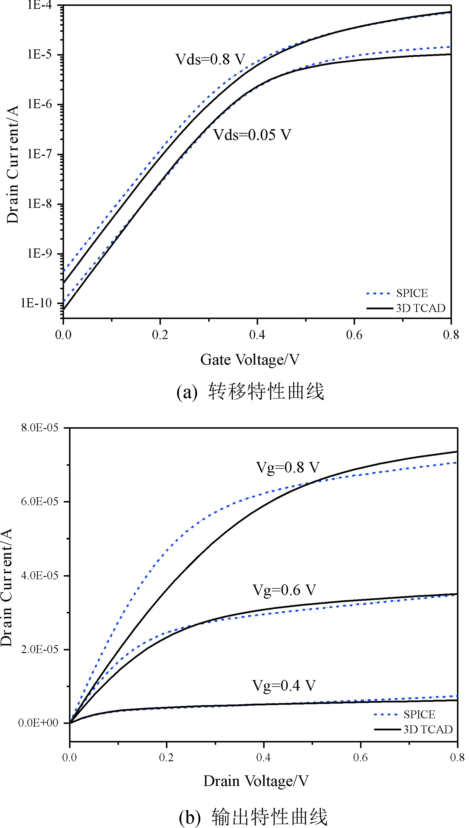
Fig. 4
I-V characteristic curves of 22 nm FDSOI NMOS device Id-Vg curves and Id-Vd curves in different bias voltage at 298 K
Fig.5
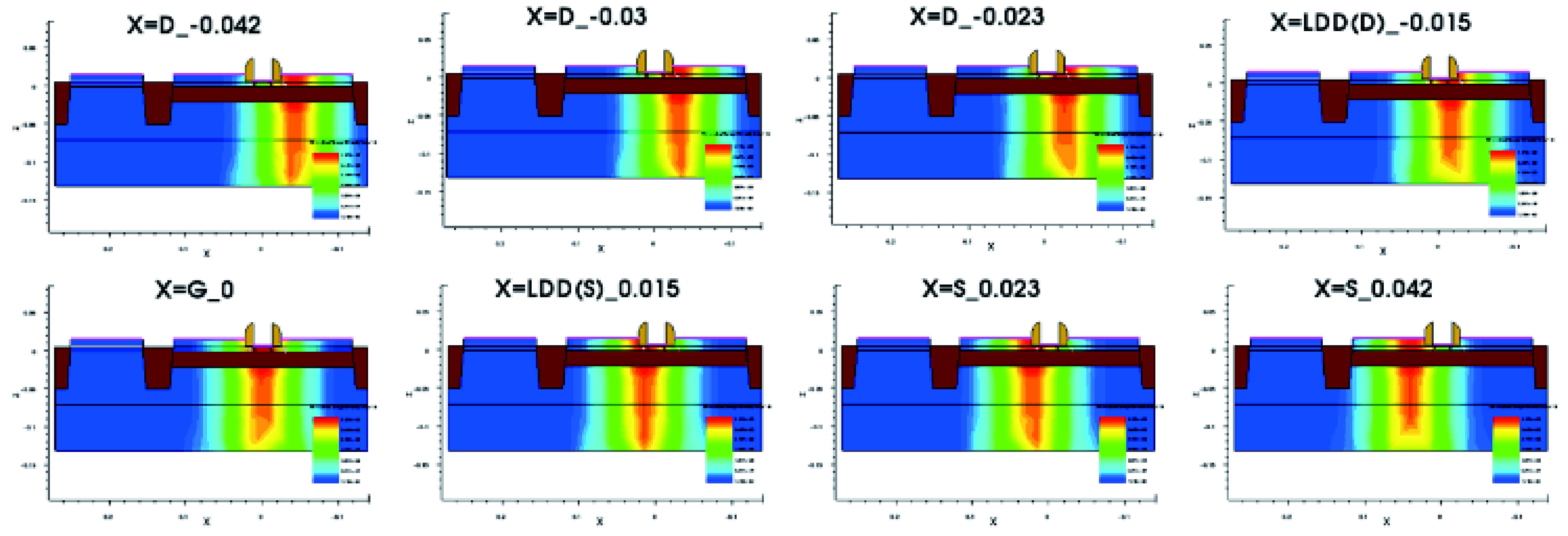
Distribution of electron-hole pairs density produced by HeavyIon model at different strike positions
Fig. 6
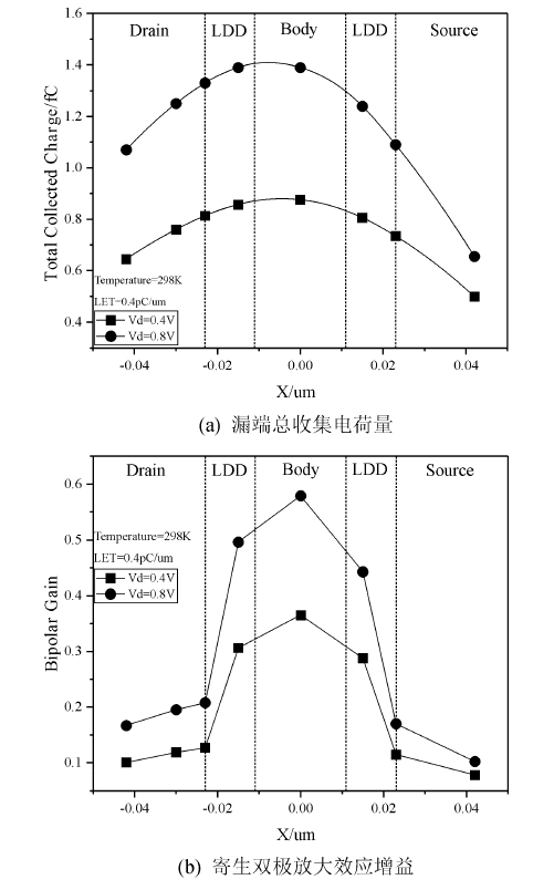
LET=0.4 pC/μm,drain total collected charge and bipolar gain in different strike location and bias voltage at 298 K
Fig. 7
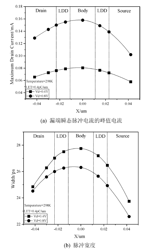
LET=0.4 pC/μm,maximum drain current and pulse width in different strike location and bias voltage at 298 K
Fig. 8
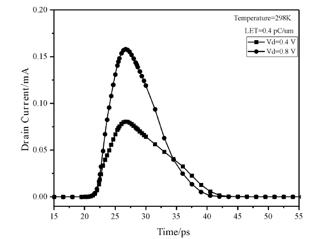
LET=0.4 pC/μm, drain transient pulse current when heavy ion strikes in the center of body region in different bias voltage at 298 K
Fig. 9
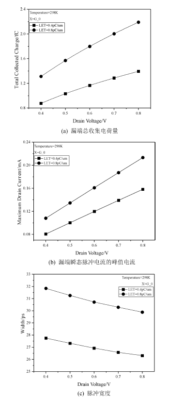
Striking at body region,drain total collected charge,maximum drain current and pulse width in different bias voltage and LET at 298 K
Fig. 10
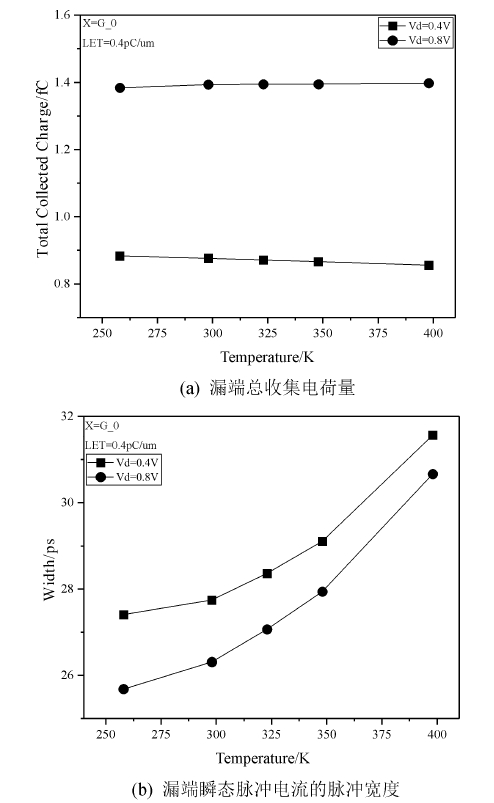
Striking at body region and LET=0.4 pC/μm,drain total collected charge and pulse width in different bias voltage and temperature