×
模态框(Modal)标题
在这里添加一些文本
Close
Close
Submit
Cancel
Confirm
×
模态框(Modal)标题
×
Home
About Journal
About Journal
Indexed in
Awards
Editorial Board
Guide for Authors
Browse
Current Issue
Just Accepted
Archive
Highlights
Topic
Most Viewed
Most Download
Most Cited
E-mail Alert
RSS
Subscribe
Download
Contact Us
Figure/Table detail
Bias voltage and temperature dependence of single-event transient in 22 nm FDSOI devices
HUANG Xiaofeng, LI Chenming, WANG Haibin, SUN Yongshu, WANG Liang, GUO Gang, WANG Xueming
Integrated Circuits and Embedded Systems
, 2024, 24(
7
): 30-36.
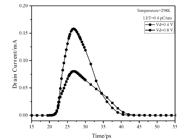
Fig. 8
LET=0.4 pC/μm, drain transient pulse current when heavy ion strikes in the center of body region in different bias voltage at 298 K
Other figure/table from this article
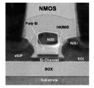
Fig. 1
Typical cross-section of 22 nm FDSOI NMOS
[
9
]
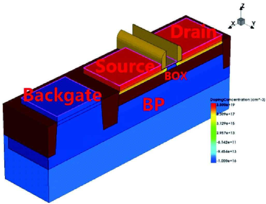
Fig. 2
22 nm FDSOI NMOS model
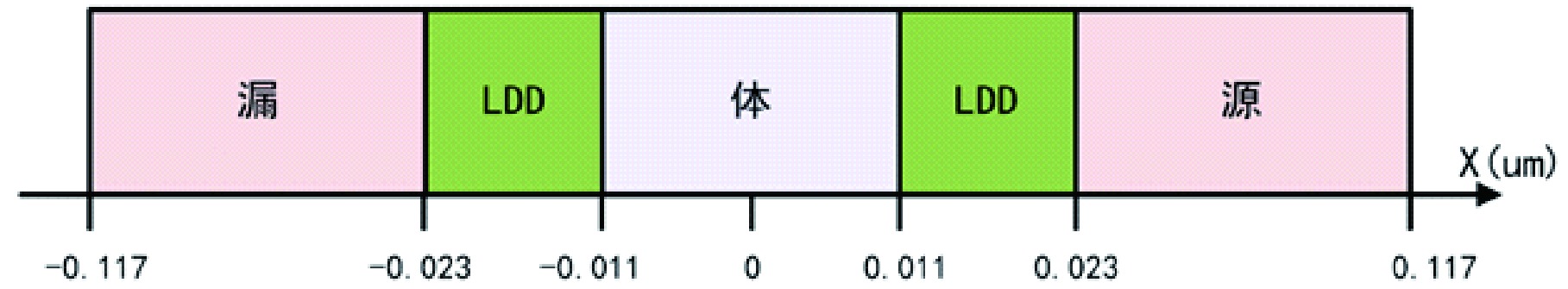
Fig. 3
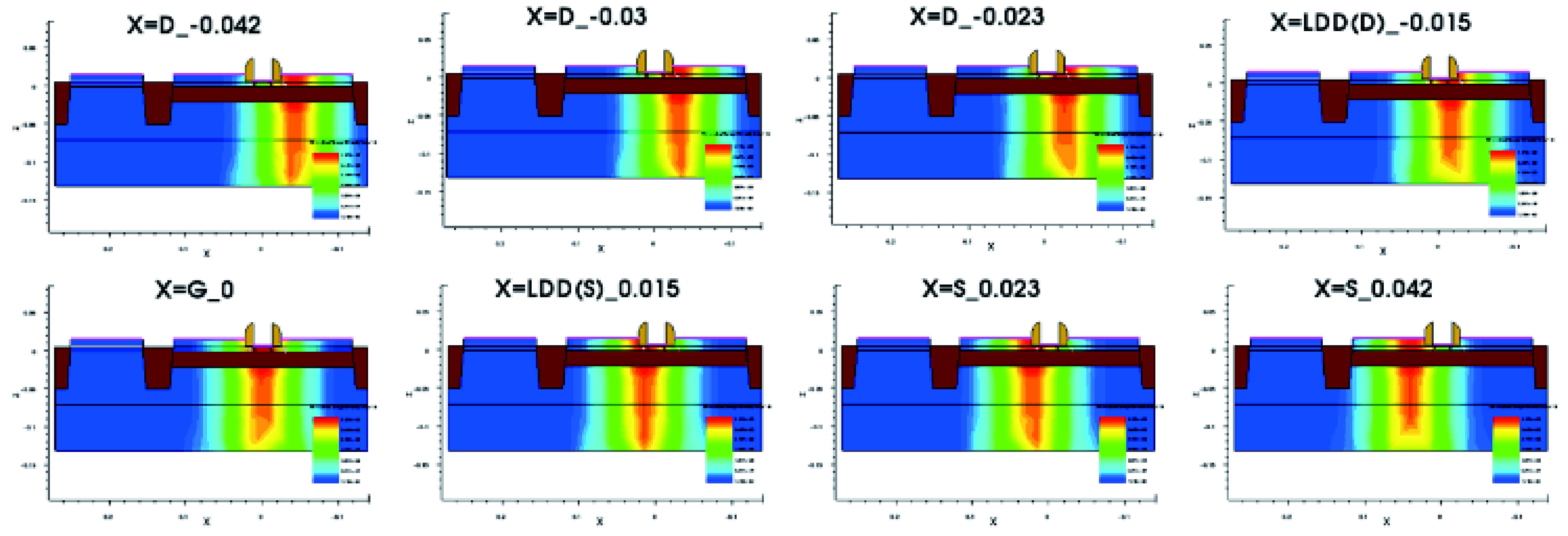
Diagram of different positions in 22 nm FDSOI NMOS model
Table 1
22 nm FDSOI NMOS model process parameters
Fig. 4
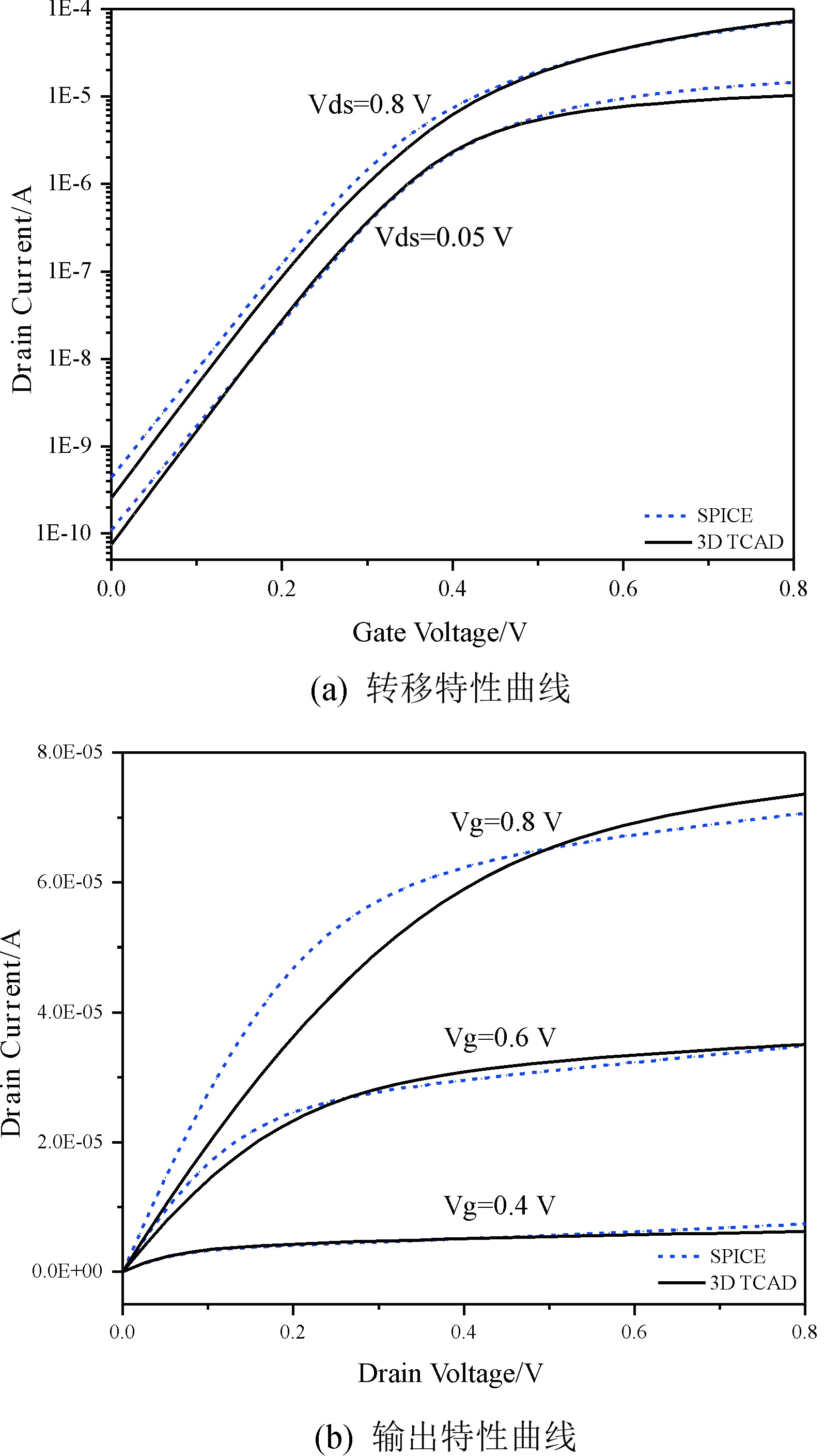
I-V characteristic curves of 22 nm FDSOI NMOS device Id-Vg curves and Id-Vd curves in different bias voltage at 298 K
Fig.5
Distribution of electron-hole pairs density produced by HeavyIon model at different strike positions
Fig. 6
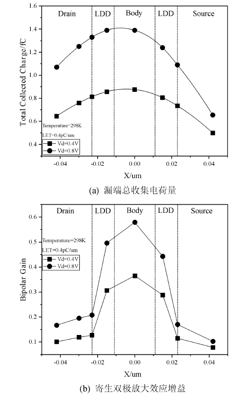
LET=0.4 pC/μm,drain total collected charge and bipolar gain in different strike location and bias voltage at 298 K
Fig. 7
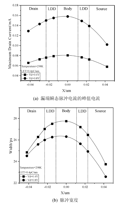
LET=0.4 pC/μm,maximum drain current and pulse width in different strike location and bias voltage at 298 K
Fig. 9
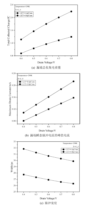
Striking at body region,drain total collected charge,maximum drain current and pulse width in different bias voltage and LET at 298 K
Fig. 10
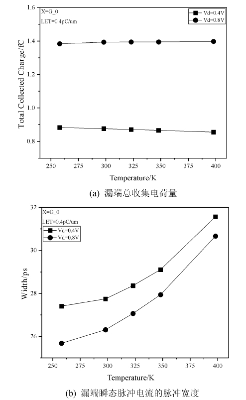
Striking at body region and LET=0.4 pC/μm,drain total collected charge and pulse width in different bias voltage and temperature