×
模态框(Modal)标题
在这里添加一些文本
Close
Close
Submit
Cancel
Confirm
×
模态框(Modal)标题
×
Home
About Journal
Editorial Board
Guide for Authors
Browse
Current Issue
Just Accepted
Archive
Highlights
Topic
Most Viewed
Most Download
Most Cited
Subscribe
Download
Editorial Policy
Publication Ethics Statement
Peer Review Policy
Contact Us
中文
Figure/Table detail
Compact modeling of I-V model for gate-all-around field effect transistors
WANG Shichun, FENG Junjie, ZHANG Baoqin, HAN Yujie, XU Chuanzhong, ZENG Xia, YU Fei
Integrated Circuits and Embedded Systems
, 2024, 24(
10
): 9-18. DOI:
10.20193/j.ices2097-4191.2024.0022
Fig. 1
3D structural diagram of GAAFET and GAAFET cross-sectional view
[
13
]
Other figure/table from this article
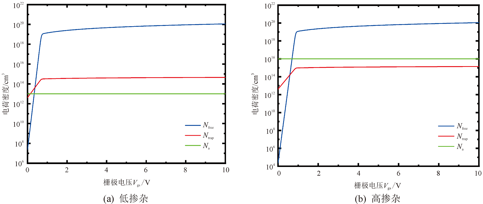
Fig. 2
Distribution of various charge densities under different doping concentrations
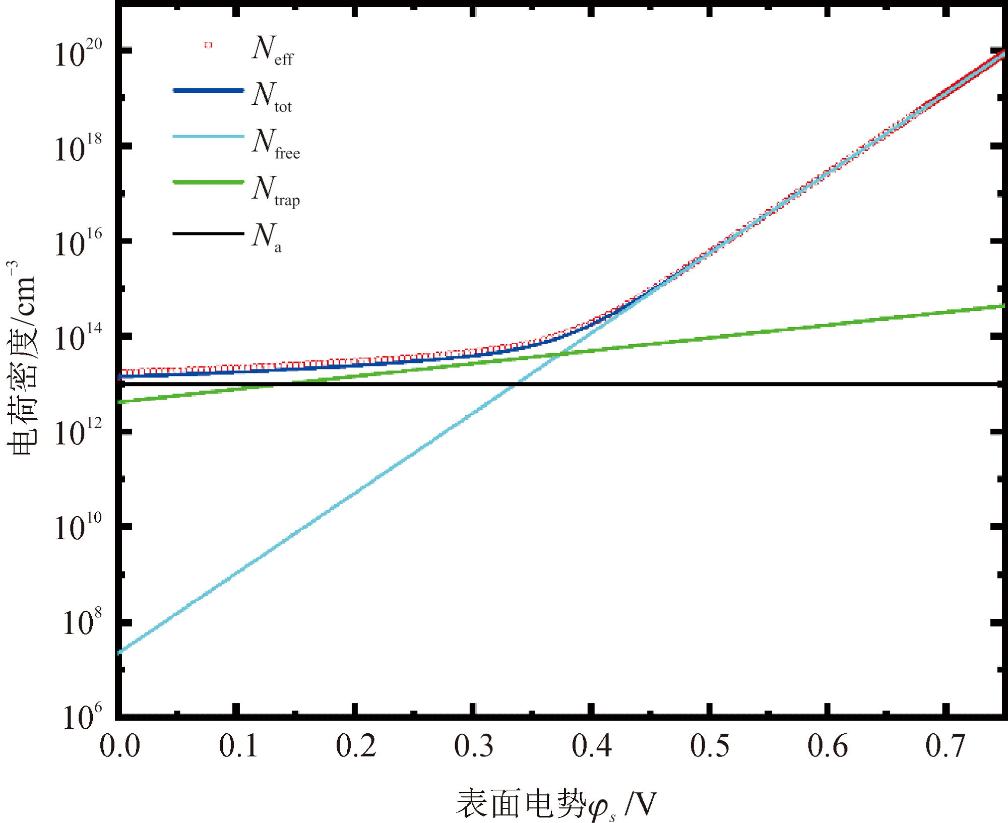
Fig. 3
The relationship curve between different types of charge density and surface potential
Fig. 4
Based on region division method
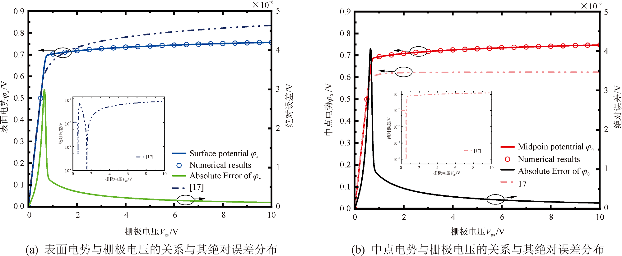
Fig. 5
Based on effective charge density method
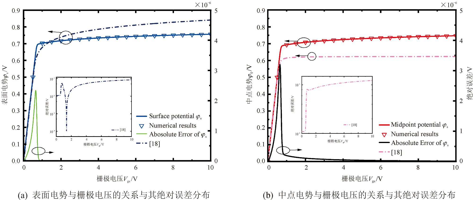
Fig. 6
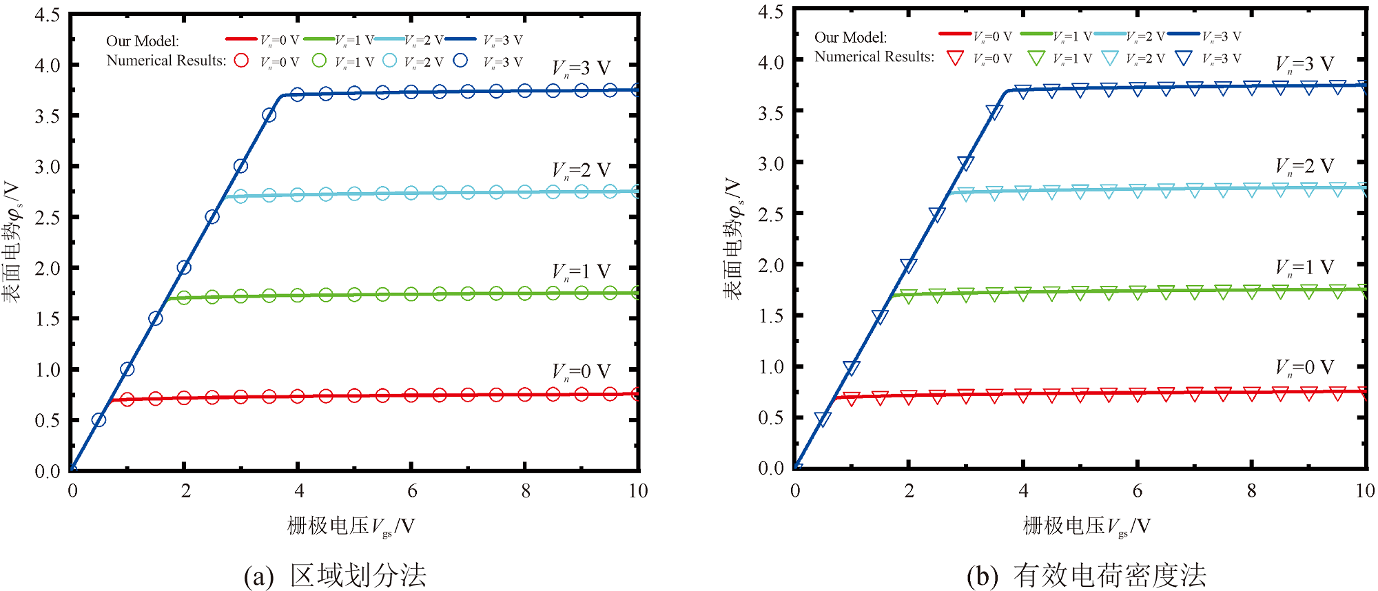
The relationship between surface potential and gate voltage under different channel voltages
Fig. 7
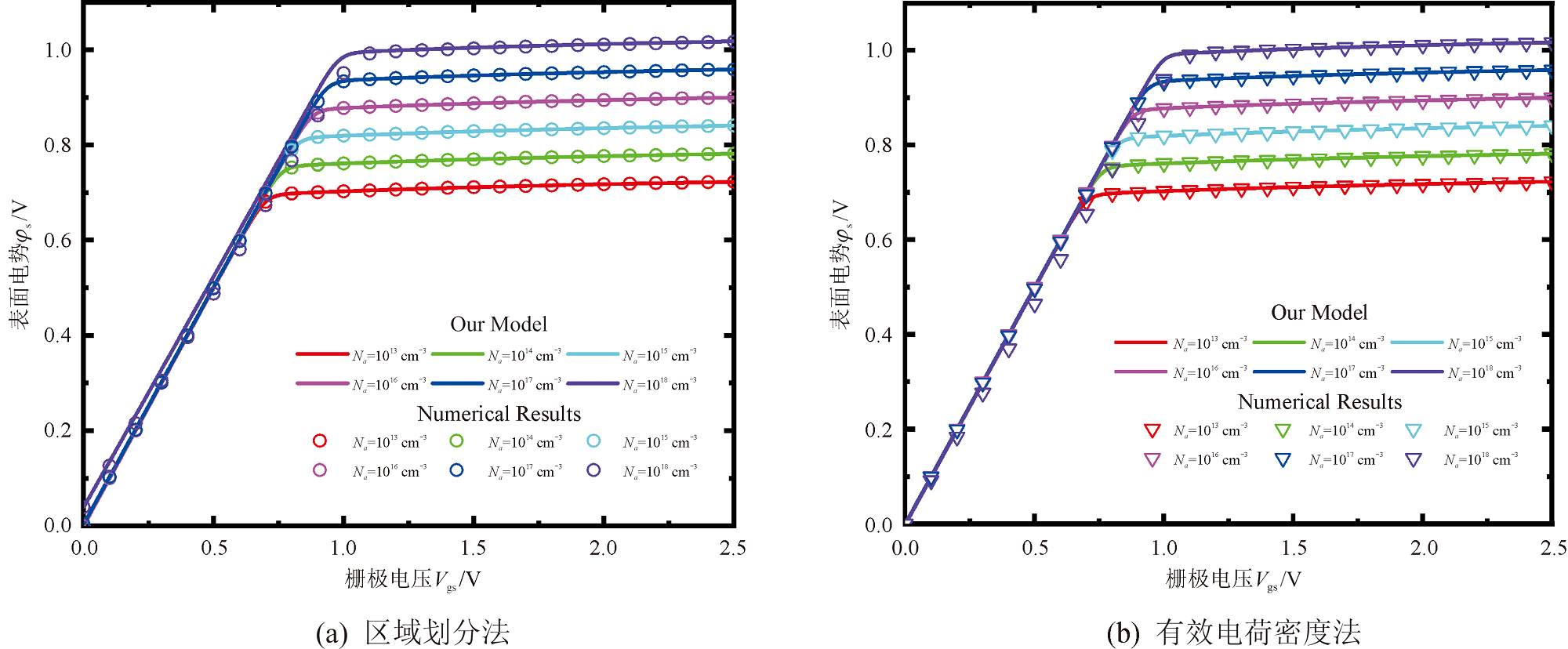
The relationship between surface potential and gate voltage under different doping concentrations
Table 1
Parameters for simulation
Fig. 8
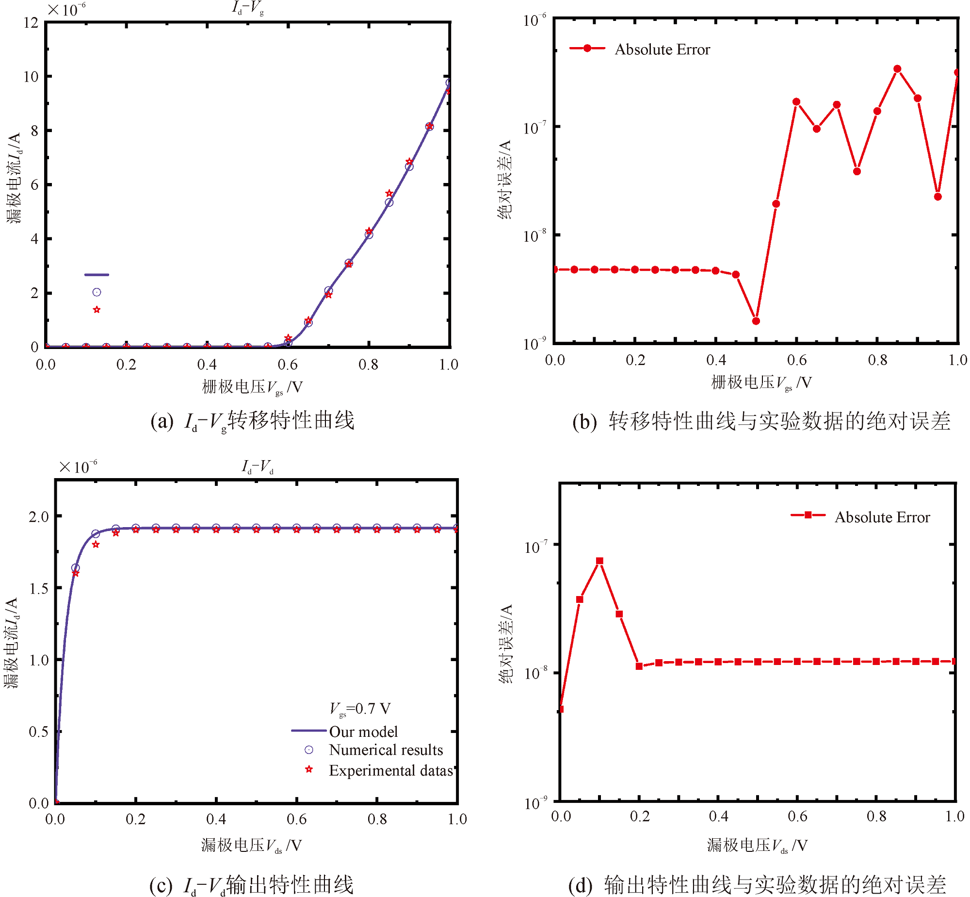
Comparison between model and experimental results based on region division method
Fig. 9
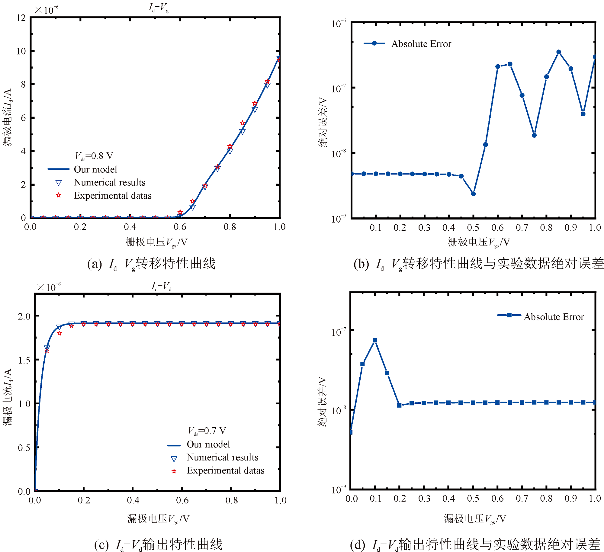
Comparison between model and experimental results based on effective charge density method