×
模态框(Modal)标题
在这里添加一些文本
Close
Close
Submit
Cancel
Confirm
×
模态框(Modal)标题
×
Home
About Journal
Editorial Board
Guide for Authors
Browse
Current Issue
Just Accepted
Archive
Highlights
Topic
Most Viewed
Most Download
Most Cited
Download
Editorial Policy
Publication Ethics Statement
Peer Review Policy
Contact Us
中文
Figure/Table detail
An efficient DDR4 debugging and testing method for SoC designs
JIANG Yande, MA Jingbo, ZHANG Guangda, WANG Dongsheng, XU Shi, PEI Bingxi, WANG Huiquan
Integrated Circuits and Embedded Systems
, 2025, 25(
11
): 31-37. DOI:
10.20193/j.ices2097-4191.2025.0069
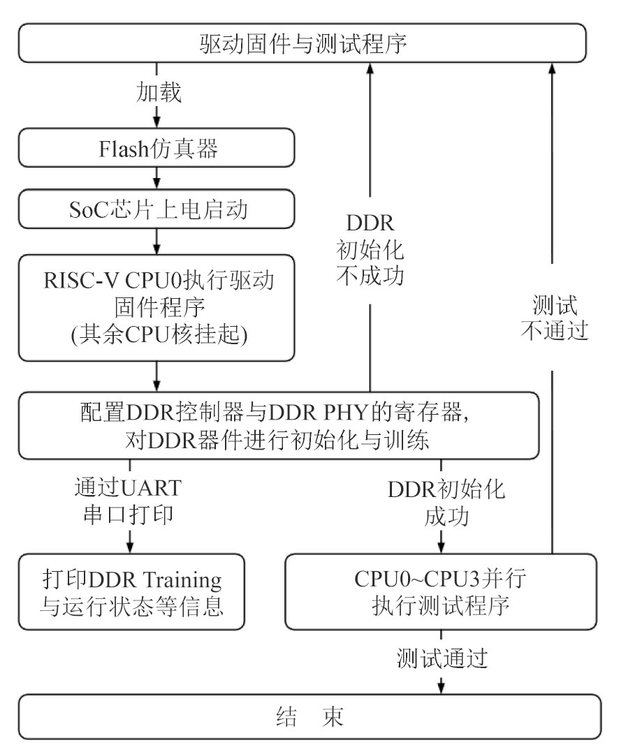
Fig. 4
DDR debugging flowchart
Other figure/table from this article
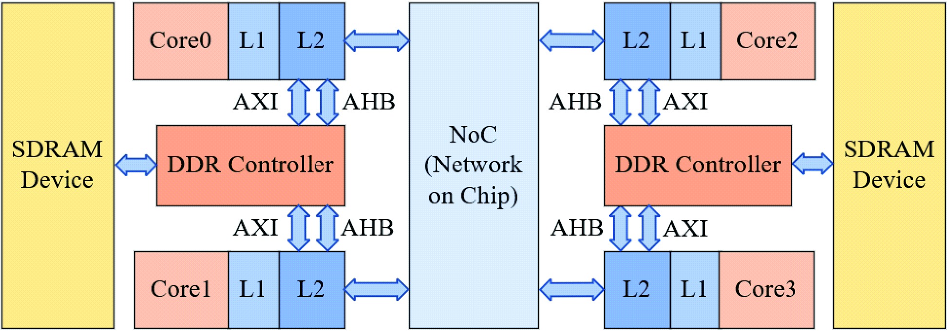
Fig. 1
The architecture diagram of a dual-channel DDR and quad-core SoC chip
Fig. 2
The SoC chip debugging framework diagram
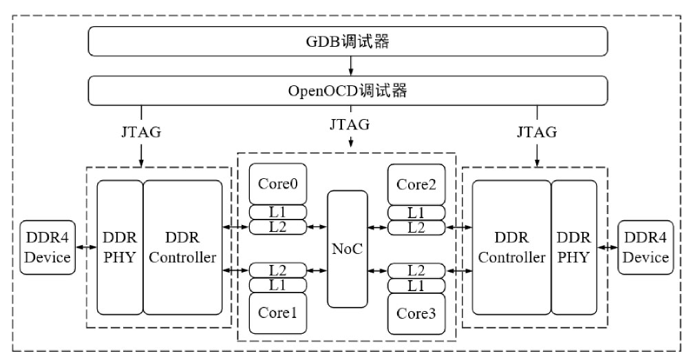
Fig. 3
The debugging framework diagram for SoC chips based on GDB and OpenOCD
Fig. 5
The structured DDR parameter configuration algorithm architecture diagram
Table 1
The DDR bare-metal level test cases and experimental results
Table 2
The DDR OS-level test cases and experimental results